Electronic Devices and Circuits Beyond CMOS Technologies
Parveen Kumar editor Balwinder Raj editor Shiromani Balmukund Rahi editor Naushad Alam editor
Format:Hardback
Publisher:John Wiley & Sons Inc
Publishing:4th Feb '27
£228.00
This title is due to be published on 4th February, and will be despatched as soon as possible.
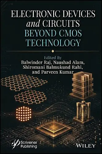
Essential for researchers and VLSI engineers navigating the post-CMOS era, this comprehensive guide delivers the theoretical models, device physics, and cutting-edge fabrication techniques needed to master nanomaterials and overcome sub-nanometer scaling challenges.
For more than five decades, complementary metal-oxide-semiconductor (CMOS) technology scaling has propelled unprecedented growth of the semiconductor industry. However, the scaling of planar silicon CMOS nanoscale technology has resulted in various short-channel effects such as velocity saturation, drain-induced barrier lowering, and threshold voltage roll-off effects, culminating in degraded device characteristics, increased leakage currents, and power dissipation. Extensive research is being carried out to address these challenges at multiple levels. This book uniquely explains nanomaterials, devices, and the analysis of their design parameters to meet the sub-nano-regime challenges beyond CMOS technologies. It comprehensively highlights conventional and novel nanomaterials, devices, and circuits, leakage current mitigation techniques, and other important trade-offs. Offering in-depth coverage of temporal degradation and interconnect delay, the book provides insight into state-of-the-art conduction mechanisms, device architecture, operation, performance evaluation, and applications of various nanoscale materials and devices in VLSI circuit design. This essential resource provides relevant theoretical frameworks that include device physics, modelling, circuit design, and the latest developments in experimental fabrication for nanoscale devices.
ISBN: 9781394466504
Dimensions: unknown
Weight: unknown
608 pages